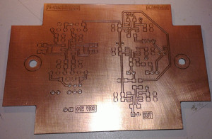
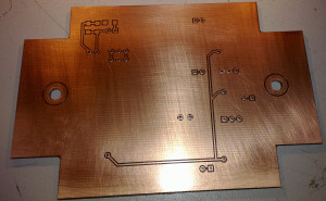
I made this PCB on the LPKF mill today:
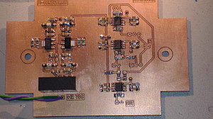
Moments later, it was populated with components:
This is a PI-controller with three op-amps. One for the P-term, one for the I-term, and one that sums P+I.
The left side of the PCB is a +/-12V power-supply consisting of a DC2DC converter, caps and EMI-filters (Murata NFE61), LM337/LM317 adjustable voltage regulators, and more caps and EMI-filters. Despite the caps and filters I'm not sure this design gives good enough +/- 12V DC supplies for instrumentation use - when the DC2DC input comes from a typical cheap "wall-wart" switch-mode PSU. Or perhaps there is direct RF/capacitive cross-talk from the wall-wart input to the op-amp circuits which shows up as noise in the signal?
The PCB is shaped to fit a Fibox enclosure.


