AD9912 DDS Test

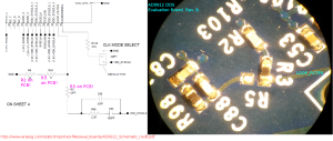
Update: it turns out the PLL filter components were not connected at all during the first tests I did 🙂 Here's a picture that compares the schematic against the actual board. When I changed the 0R resistor from position "R3" to position "R5"  the PLL started behaving much more nicely. If anyone from AD is reading - please update your documentation!

ad9912_eval_board_pll_schematic

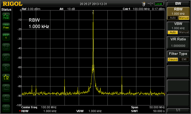
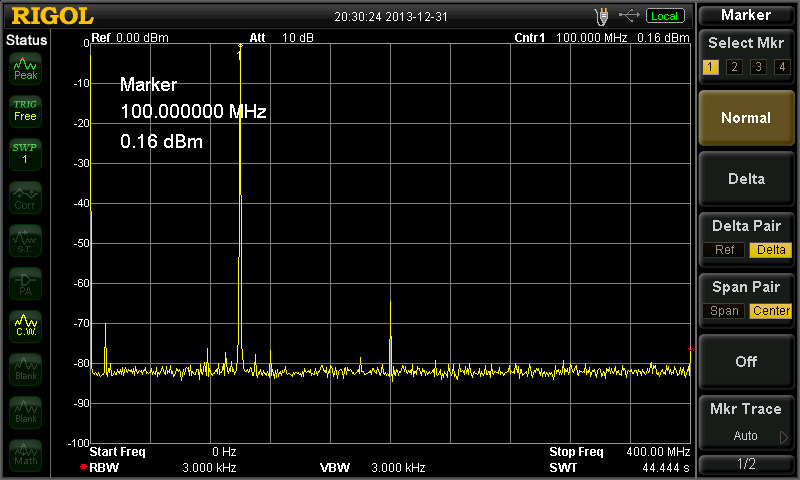
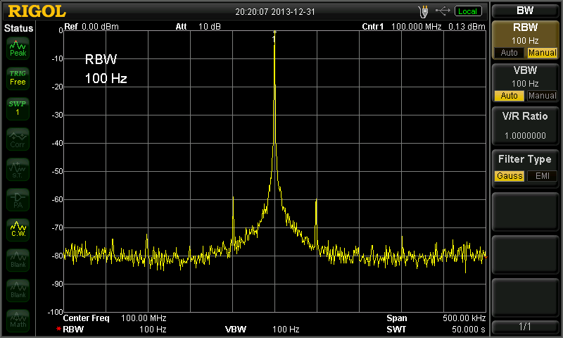
With this change, and a 66x PLL multiplier giving a 10MHz x 66 = 660 MHz SYSCLOCK I get quite nice output:

Fout100M_Span50M Fout100M_Span400M Fout100M_Span500k

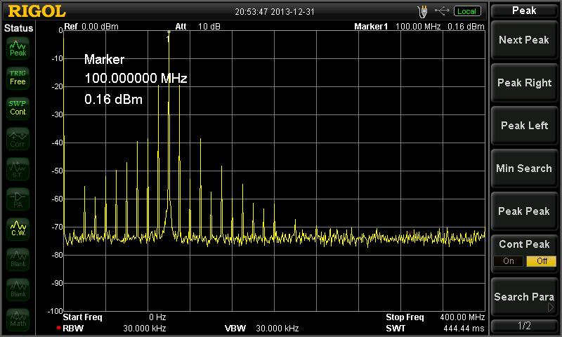
The output is set to 100 MHz and has an amplitude of ~0 dBm. There are -60 dBm spurs at +/- 50 kHz (not sure why?), -70 dBm spurs at +/- 10MHz, and a -65 dBm second harmonic at 200 MHz.

If I activate the "2x Reference" setting which detects both rising and falling edges of the input clock, and use that with a 40x PLL for a 10MHz x2 x40 = 800 MHz SYSCLOCK I still get very strong spurs at 10 MHz:

Fout100M_Span400_PLL_2x40x

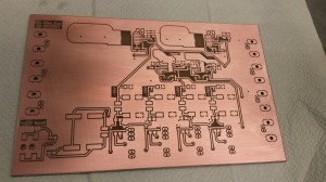
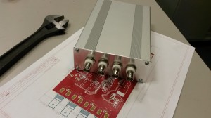
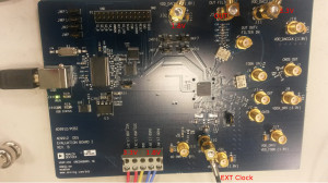
I have been testing this AD9912 DDS evaluation board:
ad9912_evkit_pcb_text

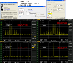
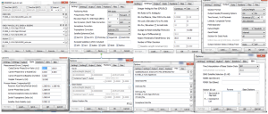
So far the results are a bit strange, with output as advertized only when no external input clock is supplied. Strange.

dds_test_2013-12-30

Comparing GPS PPP solutions

Update3 on 2014-02-20: by popular demand, screenshots of options (at least roughly correct...) used in RTKPOST to get the results shown:

rtklib_settings_2014-02-20

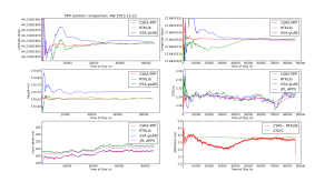
Update2: gLAB data now at 30s intervals, and an error-plot that compares CSRS to gLAB clock offset.

ppp_2013-12-25_glab


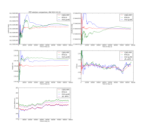
Update: using the latest RTKLib from github on Ubuntu, I now got this, with the lat/lon/height results between CSRS-PPP and RTKLib in better agreement. There is still a 4ns offset between the clock results - which curiously is about 0.5*ZTD, but this may be just a coincidence.

ppp_2013-12-25

GPS based Precise Point Positioning is used worldwide to compare clocks against each other and maintain UTC.

The idea is to connect your clock to a dual-frequency GPS receiver that collects data (in RINEX format). The RINEX data is then post-processed by using satellite orbit and clock information available (with delay) from the IGS. While normal GPS has a precision of maybe 1-10 meters (~10 ns clock offset/noise), PPP can achieve <1 cm precision (<1 ns clock offset).

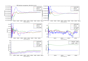
I tested a few of the PPP algorithms I found by running them on the same datafile (KAJA2900.13O) and got the results shown below.

If anyone wants to try this at home you will need from the IGS (I used RTKGet, a tool that comes with RTKLib to download these): clock data CLK file igs17624.clk, orbit data SP3 file igs17624.sp3, NAV file brdc2900.13n, antenna correction ANTEX file igs08.atx, earth rotation parameters ERP file igs17627.erp, and possibly also an ocean tide loading BLQ file available from Onsala Space Observatory.

ppp_solutions_2

The CSRS-PPP and ESA-gLAB clock offset solutions agree reasonably well, but the clock offset of the RTKLib/JPL-APPS solutions differ by  3-4 nanoseconds - which is a lot if we are using this for monitoring/steering an atomic clock. I'm not sure why this happens - if anyone knows how to reproduce the CSRS-PPP results with RTKLib please let me know!

  • CSRS-PPP is an online web-based tool that returns results by e-mail. AFAIK the same code is used by the BIPM to maintain UTC.
  • JPL-APPS is a similar web-service by NASA.
  • ESA gLAB and RTKLib are open-source software packages for GPS/GNSS processing.

See also: A Comparison of Free GPS Online Post-Processing Services


Optics adapter plate

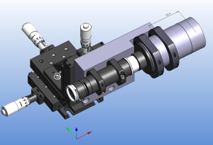
Mechanical design for an optics assembly:
pmt_optics_1

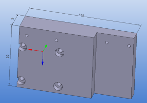
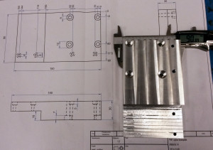
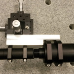
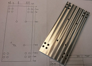
I made an adapter plate between the XYZ translation stage and the 2"/1" lens-rings. The XYZ stage has a 50 mm x 50 mm M6 thread pattern, and the optics are mounted on a straight line with M4 screws through the adapter plate. M6 countersink is 12mm diameter 7mm deep, while the M4 countersink is 8mm diameter and 5mm deep.

adapter_plate adapter_plate_machined

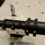
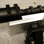
In real life this looks almost like the CAD model:

Butterfly laser diode mount

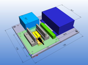
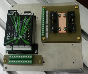
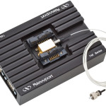
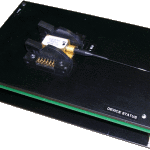
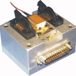
We've put together a few of these butterfly laser-diode mount + driver combos. It combines a heat-sinked butterfly mounted laser-diode with a current/temperature controller by Wavelength Electronics. The assembly is low enough to fit into a 1U (~44 mm) high 19" rack-enclosure.
bfly_mount_v1_assembly_2013sep3 bfly_mount_v2_assembled

The 14-pin laser-package (yellow) is held in place by ZIF clamps/sockets 5253-100-07S (standard) and 5253-100-07R (reverse) from from Azimuth Electronics (grey in the CAD drawing, black in real life). The Wavelength Electronics LDTC driver controls both the laser current and temperature using the laser's own on-board TEC and thermistor. The base-plate has additional room for a heatsink and a fan, but so far I think nobody has used this feature. Semiconductor lasers have about 30% efficiency, so with anything under 1 W of optical output the dissipated heat should stay below 3-5 W.

The metal parts are an aluminium base-plate (see bfly_mount_v1_plate_2013aug26 and the newer bfly_mount_v2_plate_2013nov1). A copper riser-block (bfly_mount_v1_riser-block_2013aug26) sits on top of the base-plate and provides good heat-conduction from the laser package to the base-plate. The riser-block and the laser are bolted together with M2.5 bolts/screws (allen-bolts would be more stylish - I know!). I also made a mechanical drawing for the PCB bfly_mount_v1_pcb_drawing.

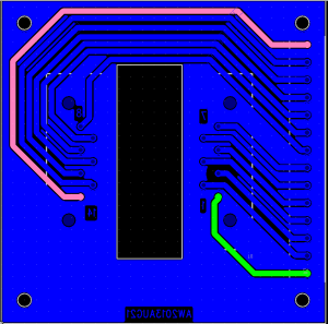
The PCB has no electronics on it (see bfly_mount_v1_schematic_2013sep3), the pins from the Azimuth sockets are just routed to 150 mil pitch screw terminals.

bfly_mount_v1_pcb_2013sep3bfly_mount_v1_pcb_assembled

See also gerbers for manufacturing: butterfly_pcb_v1_camfiles or the slightly modified version dated 2013-11-14 butterfly_v3_camfiles

screwterminal_pcb

There's an additional mini-pcb for screw-terminals on the input side of the LDTC controller. screwterminal_camfiles_2013-09-12

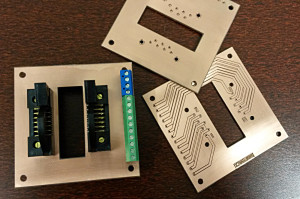
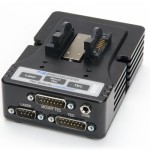
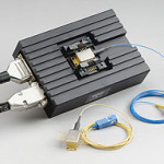
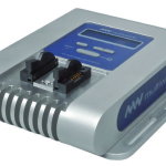
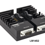
Our in-house design won't win any prizes for design or style, but it does the job. Here are a few pictures of commercial butterfly mounts. Some combine the current/temperature driver with the mount, others just have D-sub connectors for external current/temperature controllers.

GPIB on Linux

Update 2015 June: additions for Ubuntu 14.04LTS (where a symbolic link is required), and for the NI-USB-B dongle (which needs firmware loading). See also: Using the National Instruments GPIB-USB-B on linux

Notes on how to use GPIB from python on Ubuntu 12.04LTS. Tested with National Instruments USB-GPIB device and a recently bought NI GPIB PCI-E card.

  • Get linux-gpib source from http://sourceforge.net/projects/linux-gpib/
  • Building the python bindings requires libboost-python (and maybe libboost-python-dev)
  • build linux-gpib by running: ./configure, make, sudo make install
  • edit /etc/gpib.conf to fit your hardware. The default config board_type = "ni_pci" seems to work with the NI PCI-E card. For the USB-GPIB device we need board_type = "ni_usb_b"
  • load the kernel module, for the PCI-E card this is sudo modprobe tnt4882, for the USB-dongle this is sudo modprobe ni_usb_gpib
  • On Ubuntu 14.04LTS the library that gpib_config is linked against is installed in a location where the binary doesn't find it. The fix is to add a symbolic link in /lib/
    /lib$ sudo ln -s /usr/local/lib/libgpib.so.0 libgpib.so.0
  • configure: sudo gpib_config --minor 0 this reads and parses /etc/gpib.conf so it needs to be re-done if something is changed in gpib.conf
  • If gpib_config fails, and you have the older/slower NI-USB-B dongle, then you need to first load the firmware. This seems to not be required with the newer NI-USB-HS (to be confirmed?). Firmware loading requires fxload and the firmware from http://linux-gpib.sourceforge.net/firmware/. Find out where your USB-dongle is with lsusb and then load the firmware with something like:
    fxload -D /proc/bus/usb/001/002 -I niusbb_firmware.hex -s niusbb_loader.hex where you replace /001/002 with the numbers for your USB device. Now gpib_config should work.
  • By default only members of the gpib-group can use gpib, and only root has access to /etc/gpib0. If we want normal users to use gpib, add them to the gpib group (on Ubuntu the graphical user&group editor is gnome-system-tools)
  • Test!
    note: If "import gpib" fails in python you might have forgotten to install libboost-python before building linux-gpib. Python bindings will not be built&installed unless you have libboost-python.

I have two devices, so I've configured them like this in gpib.conf

/* agilent mux/dmm */
device {
	minor = 0 /* first gpib-card/usb-dongle */
	name = "dmm"
	pad = 8 /* primary address, configure on instrument front-panel*/
	sad = 0 /* secondary address, always zero? */
}
/* kikusui psu controller */
device {
        minor = 0
        name = "kikusui"
        pad = 1
        sad = 0
}

And now we can try some python:

1
2
3
4
5
6
7
8
9
10
11
12
13
14
15
16
17
18
19
20
import gpib
import time
dmm= gpib.find("dmm") # define in /etc/gpib.conf
kik= gpib.find("kikusui")
 
def query(handle, command, numbytes=100):
	gpib.write(handle,command)
	time.sleep(0.1)
	response = gpib.read(handle,numbytes)
	return response
 
print query(dmm,"*IDN?")
print query(kik,"*IDN?")
 
gpib.close(dmm)
gpib.close(kik)
 
# output:
# HEWLETT-PACKARD,34970A,0,13-2-2
# KIKUSUI ELECTRONICS CORP.,PIA4830,0,2.20

DC-Bias Amplifier

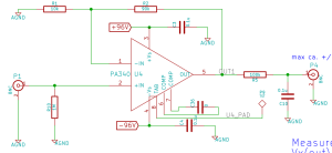
I've put together the first version of a DC-bias amplifier used for applying four DC-voltages to the trim electrodes of an ion trap. The axial voltages required are low, and they are applied symmetrically as +Vz and -Vz. The transverse voltages (X and Y) however can be as high as 100 V. Two high-voltage op-amps PA340CC are used for the X and Y channels, while the -Z and +Z output voltages are produced by two OPA454 op-amps. The amplifier has three +/-10 V inputs (Vx, Vy, Vz), and produces four outputs designed to be 10*Vx, 10*Vy, -Vz, and +Vz.

The amplifier circuit itself is very simple with the two PA340CC's in non-inverting configuration with a gain of 10, and the two OPA454's in inverting configuration, connected in series, with a gain of 1. The bandwidth requirement is very low, and the load should be equivalent to an open circuit - hence high 100k output resistor and a cap producing a 16 Hz low-pass filter on the output
schematic_pic

See full schematic as PDF: bias_amp_v0

The high-voltage DC-rails for the op-amps are produced by connecting four +/-24 V DC-to-DC converters in series. This allows powering the amplifier from a single +12VDC powersupply-brick, and in theory produces +/-48 V for the lower-voltage op-amps and +/-96 V for the high-voltage op-amps.

One issue with DC-to-DC converters is that they produce both differential and common-mode noise on the output. Conventional filter-caps or Pi-filtering removes the differential noise but does nothing to the common-mode noise. A common mode choke and/or filtering capacitors across the isolation-barrier to the input-side ground are required to remove the common-mode noise. Here's a picture from a Murata app-note that explains the idea:
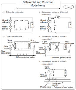
diff_common_noise

The components fit comfortably on a 100mm by 160mm PCB like this:
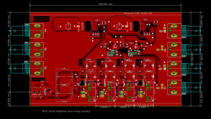
pcb_pic
Only top Cu-layer shown. Why doesn't Kicad have built-in PDF export for the PCB-editor (like in the schematic-editor)?

Gerber and Excellon files from Kicad worked without problems with CircuitCAM for producing toolpaths for BoardMaster that runs our LPKF PCB mill. The PCB after milling, rubbed with steel-wool, cleaned with isopropanol, and then coated with PRF202.
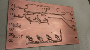
pcb_milled_bottompcb_milled_top

Components soldered, and board fit into an enclosure (Multicomp MCRECS160):
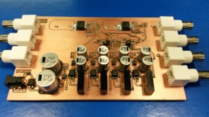
pcb_solderedpcb_boxed

When powered up the DC-rails measured slightly lower voltages than expected. I got -89V, -44V, +44V, and +89V. The no-load input current was surprisingly high at 190mA. The dc-to-dc converters have a no-load spec of 20mA, so this explains about half of the measured current. The op-amps have a quiescent current of 3.2 mA @ +/48V for OPA454 and 2.2 mA @ +/-96V for PA340. So the 'middle' DC-to-DC converters that power all four op-amps should have 2*(3.2+2.2)= 10.8mA load at 48V and the 'side' converters only 2*3.2=6.4mA at 48V. That's 17.2 mA at 48V together, which should correspond to 84 mA at 12V if we trust the 82% efficiency number from the datasheet. So we can explain 80mA as no-load current and 84 mA from the quiescent current of the op-amps. That's 164 mA together, which is about 85% of the 190mA number shown by the powersupply. If my reasoning here is way off please comment below!

Initial measurements shows that the outputs behave roughly as designed. The high-voltage outputs max out at about +/- 85 V. Note that the 10 MOhm input of a DMM measures only 99% of the actual output voltage, due to the high 100k output impedance of the amplifier.
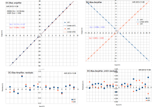
bias_amp

The frequency response is completely dominated by the 16 Hz low-pass RC-filter on the output, although the op-amps have unity-gain bandwidths of ~10 and ~2 MHz.
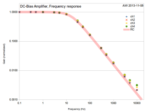
bias_amp_fresponse

Notes and comments:

  • This was the first board I designed with Kicad. It works rather well, and new enhancements are already on the way. The export of a netlist from the schematic-editor to the PCB-editor could be a bit smoother, and the footprint assignment should probably be done in the schematic-editor and the current CvPCB footprint-assignment bypassed.
  • I used quite conservative design rules(mils): clearance 16, track 25, via 55, via drl 35. This seems to work quite well. The clearance could be reduced down towards 8 mils which is the minimum isolation clearance the PCB-mill can produce. Kicad automatically enforces clearance and via design rules interactively while routing the tracks - this is probably good once you get used to it.
  • I messed up the polarity of the diode footprints - should be fixed if a second version is built.
  • Linear regulators could be added on the DC-rails, after the pi-filters. Or perhaps a shunt regulator on the high-voltage rails.
  • With no load the op-amps don't seem to heat up. So the heatsink copper areas may not be required.
  • The BNC-footprint "BNC_Socket_TYCO-AMP_LargePads_RevA" has a quite large drill-spec for the mounting holes, could be reduced from 2.2mm to 2.1 or 2.0mm. The signal pin holes are also quite close to the large mounting holes. they could be moved further away by maybe 0.5 mm.
  • I used kapton tape on the sides of the board, to insulate AGND from the aluminium case. Not sure what voltage the case should be at( +12V input ground?).
Riser Block

I cranked out this 27mm high riser-block from a piece of 35x100 mm aluminium bar today.

The 6mm holes in the corners are for attaching the block to a standard breadboard or optical table that has M6 threads on a 25mm pitch. There are four holes in each corner in a 12.5-by-12.5mm square pattern. These allow attaching the block with 12.5mm 'resolution' both along X and Y.

The middle M6 tapped holes are for attaching to a translation stage. The stage is old with a weird 34x92mm bolt pattern.

riser_block_2013nov8

Strontium ion(s) trapped!


A major milestone towards the ion clock was reached today: we trapped the first Strontium ions!

This involves first heating a dispenser that contains Strontium atoms with about 4-5 W (4 A and 1 V). The atoms that fly out of the dispenser are then photoionized using two blue lasers, one at 461 nm and another at 405 nm (we use a laser from a blue-ray drive for this!). We now have Sr+ ions that can be trapped in a Paul trap. A high-voltage (300 Vpp) ~10 MHz sine-wave is applied to the electrodes of the trap. Another blue laser at 422 nm is then used both for laser-cooling and as a means to detect the ion. What we see in the video is the ion fluorescence at 422 nm when it jumps down to the ground state from an excited state. The excited state can also decay into a dark state and we need a re-pump laser at 1092 nm to keep the ion in the Doppler cooling cycle. The fluorescence emitted from one or a few ions is very weak, and we used an image-intensifier and a CCD camera with 500 ms to 1 s exposure time for this video.

The camera software produces FITS frames as output. I used these commands to make the video:

mogrify -format png *.fts   # convert to PNG
mogrify -crop "640x480+436+315"  +repage *.png  # crop to the interesting area
mogrify -contrast-stretch 10x100 *.png # improve contrast
ffmpeg -r 3 -f image2 -i 'myframes_%02d.png' -qscale 1 'video.avi'

On the last line "3" is the desired frame-rate of the output. I then concatenated a few of these videos together with

mencoder video1.avi video2.avi  -mf fps=3 -oac copy -of lavf  -ovc copy 
-lavcopts aglobal=1:vglobal=1:coder=0:vcodec=mpeg4:vbitrate=4500 -vf scale=1280:720  -o output2.mp4

Strontium 461nm absorption/fluorescence revisited

This is the same experiment we did back in April, but now "in-situ" in another vacuum system that houses our RF endcap trap. The thin ray of light that slowly switches on and off is a 461nm blue laser-beam that excites Strontium atoms that fly in from the lower right corner of the picture. The on/off switching happens because we slowly scan the laser frequency back and forth and as a result different parts of the atom-stream absorb and emit.

Next stop: ionizing the atoms and trapping a single ion in the RF trap.

See also:

NTP shared-memory refclock driver for White Rabbit SPEC

ntp_graph

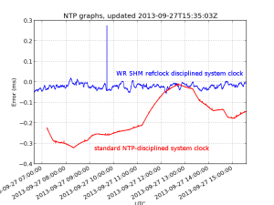
I've been playing with White Rabbit hardware at work. White Rabbit uses a combination of SyncE and PTP to perform very precise (<1 ns) time-distribution.

The standard low-precision way to distribute time is NTP. I hacked together a very experimental "Type 28" NTP refclock driver that reads the WR-time from SPEC shared memory and writes it to another location in shared memory where NTP expects it. Code over here: https://github.com/aewallin/ptp2ntpd

The graph shows system clock variations compared to WR-time (which we assume is very accurate) for a computer with the WR-refclock driver enabled (blue trace, minpoll 16 s), and another computer where the system clock is kept on time using standard NTP (I just added some servers to ntpd.conf, no other settings changed from default Ubuntu 12.04LTS). The WR-disciplined clock stays within maybe 50 microseconds with no net drift during the ~9 hour measurement, but the trace is quite jumpy. The NTP-disciplined clock wanders around much more (300 us) but the trace is smoother.