Agilent 34901A and 34907A breakout boards

Update 2015-09-16:  Csaba Toth sent a picture of his front-panel for these breakout boards. Very nice finish with text/graphics on the 19" rack panel!

20150908_231719

Front

Update 2015-05-15: Files for PCB manufacturing: top, bottom, outline Gerber files, and Excellon drill files.

When opened with e.g. gerberview they should look like this:
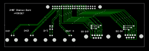
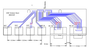
breakout2 breakoutThe connector placement is shown here (sorry I don't have a drawing for the one with 20 BNC connectors):

breakout2_connectors

A frustratingly large portion of any electronics or control system build has to do with cables and connectors. So here we go...

I'm using an Agilent 34970A datalogger/switch, which is a 6.5 digit (~22 bit) multimeter that takes up to three plug-in modules with various functions.
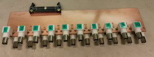
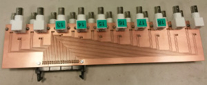
I'm using one 34901A module for 20 channels of DC voltage inputs. On the module there are 40 screw-terminals for these voltages which I have connected to a 40-pin ribbon cable that connects to this breakout board with 20 BNC connectors. Our PCB-mill can do 300mm long PCBs, which is just long enough for this board if the BNC connectors are interleaved on different sides of the board. Mounting BNC-connectors right next to each other on the same side is bad idea anyway as the connectors on the cables will not fit that closely. It should be possible to mount the whole thing in a 1U 19" rack panel.

34901A_breakout_top_2013sep 34901A_breakout_bottom_2013sep

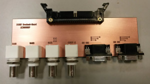
For controlling the TEC drive I need analog outputs, provided by a 34907A module. Again I'm using a 40-pin ribbon cable from the screw-terminals on the module, and the breakout board has four BNC connectors: Two DAC outputs, one counter input, and a gate input for the counter). Additionally there are two 8-bit digital I/O ports which are routed to two DB9 connectors on the breakout board.

34907A_breakout_top_2013sep

TEC Drive in enclosure

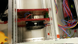
The TEC drive I have been working on is now mounted as a plug-in card in a 3U 19" rack enclosure like this:

tec_drive_rack_mounted

The card next to the TEC drive holds an 80 mm fan which helps cool the heatsinked linear regulators and the linear H-bridge that drives the TEC.

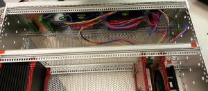
tec_drive_rack_backpanel

The back of the 19" rack enclosure holds two TRACO POWER PSUs that produce +/-5 V at max 4 A and +/-15 V at max 667 mA. An IEC power-entry module containing the IEC-connector, a fuse, and a power switch is visible far right. Far left is a small PCB for distributing +/-15 V to other cards in the same enclosure.

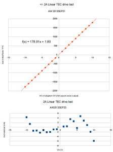
Added cooling allows testing the drive at the max input level of +/-10 V, which should produce (roughly) an output of +/-2 A.

tec_drive_test_2013sep23

The output current follows 179 mA/V * Vin + 1.8 mA with a maximum nonlinearity of about 6 mA (0.3% of full-scale). Despite the fan-cooling the transistors still get quite hot and staying below 1 A output in continuous operation is probably a good idea.

TEC-Drive heat sinks

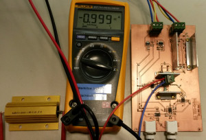
tec-drive_heatsinks_2013sep4

I made four heat sinks from aluminium L-profile for the linear TEC drive. Two 30 mm long for each side of the H-bridge (middle), and two 50 mm long for the voltage regulators(top right).

The regulators take 5 V input and produce 2 V, so they each dissipate 3V *ITEC Watts. The H-bridge dissipation is load-dependent, but for a low resistance load the dissipation is almost 2V*ITEC Watts. Here I am using a resistor (lower left) as a dummy load.

I tested the drive at 1 A for a few minutes, and the heat sinks do get quite warm. For continuous use at 2 A I think a fan will be required.

TEC-Drive prototype

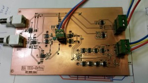
I've been assembling and testing this PCB over the past few days:

tec-drive_prototype_2013_08_01

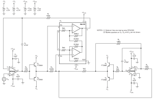
It's a linear +/-2 A voltage-to-current amplifier meant for driving a constant current through a Thermoelectric Cooler (TEC). The circuit is (loosely) based on a 2001 Burr-Brown/TI application note "SBEA001 - Optoelectronics Circuit Collection".

sbea001_tec-drive_v3

Description: U1 drives one half of the H-bridge (Q1 and Q3) based on a feedback signal which is the amplified (U3) voltage drop across a current-sensing resistor (R4). The other H-bridge half (Q2 and Q4) is driven by an inverting amplifier (U2) which forces the other end of the TEC symmetrically, inverted, to follow the output from U1.

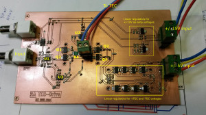
Here's how these things look on the PCB:

tecdrive_drawing

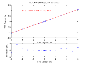
After some assembly, bugfixing, and tweaking I measured a DC transfer function like this:

tec-current_vs_input_voltage_2013aug1

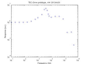
I am happy with the small offset of <0.2 mA and the linearity seems good. There is a rather large gain-error since the design-goal was 200 mA/V and the measured sensitivity is 179 mA/V. The AC frequency response is quite ugly with a high peak at a few kHz. In the time-domain this shows up as severe ringing when driven by a square-wave input. (aside: the SBEA001 application note shows a SPICE-simulated frequency response up to MHz frequencies - theory/simulation and practice differ a lot in this case!).

tec-drive_f-response_2013aug1

Things learned so far:

  • The original design used OPA353 op-amps. I had assumed these will work with bipolar +/-12 V supplies and the output swing would be close to +/-10 V. Not so! (the OPA353 is a single-supply op-amp). I used TL071 op-amps instead and they seem to work.
  • Bypass capacitors close to the collectors of Q1-Q4 are essential (but not shown in the circuit-diagram!). The feedback loop would go mad with oscillations without 1 uF caps placed close to Q1-Q4.
  • Q1-Q4 (and the linear regulators) will require heatsinking for >1 A currents.
  • The current-sensing instrumentation amplifier U3 (I used an AD8221 instead of the INA155 in the application note) is probably the most sensitive part of this circuit. I added 200 Ohm series resistors on the inputs, as well as low-pass filter capacitors (100 nF) to ground on both + and - inputs. This seems to have a calming effect on noise/oscillation of the feedback loop.
  • This kind of push-pull power stage shows significant cross-over distortion when the input signal crosses zero. Here the op-amp that drives the bases of the transistors needs to slew quickly either up or down in order to turn off one transistor and turn on the other one.

If all goes well this TEC-drive will be part of a temperature control system consisting of about five different PCBs or circuits:

  • Digital controller. Talks over SPI to DAC and ADC cards. Runs PID and/or feed-forward algorithm on real-time OS to keep temperature steady.
  • ADC-Card. Reads +/-10 V input voltage at 24-bit resolution and 1-100 samples/s speed.
  • DAC-Card. Outputs +/-10 V voltages as input to TEC-drive. 1 sample/s speed is sufficient.
  • Temperature-sensor frontend. Converts pt100 (or alternatively 10k NTC) resistance change into +/-10 V output for ADC. Previous blog posts here and here.
  • TEC-Drive (this PCB). Converts +/-10 V input from DAC into a +/-2 A constant current through the TEC.

NTP time measurement

NTP_time_2013jul26

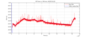
Here's a plot of the time error between the standard unix system-time, kept on time using NTP, and a much more accurate PTP-server based on White Rabbit that runs on a fancy FPGA-based network-card.

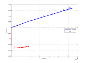
Note that without NTP a typical computer clock will be off by 10 ppm (parts-per-million) or more. This particular one measured about 40 ppm error in free-running mode (no NTP). That means during the duration of this 16e4 s measurement we'd be off by about 640 milliseconds (way off the chart) without NTP. With NTP the error seems to stay within 3 milliseconds or so. The offset of -16 milliseconds is not that accurately measured and could be caused by a number of things.

freerunning_vs_ntp_2013jul26

pt100 frontend

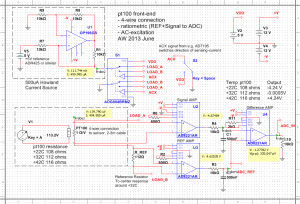
Here's a sketch for a pt100/RTD frontend circuit.

pt100_frontend_2013june11

There are a couple of ideas here which should improve precision:

  • 4-wire connection, to eliminate lead-resistance effects
  • Ratiometric measurement (both a reference and the signal go to the ADC). This should minimize effects from fluctuations in the sensing current.
  • AC-excitation. The sensing current can be reversed with at TTL logic signal. Some ADC chips have an output for this, and they average the measurement done with current flowing in both directions. This eliminates effects from DC-offsets (thermovoltages etc).
  • The circuit is centered around a particular temperature (here +32C) and the signals amplified so a twenty degree span of +22C to +42C should give about +/- 4 V output.

NI Multisim file for this: pt100_sensor_circuit_v3

Crimp Clamp Tool

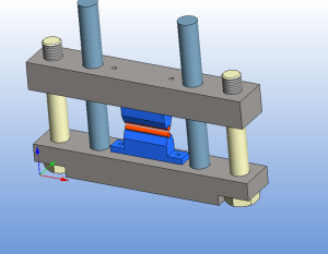
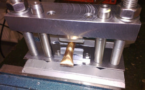
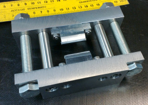
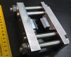
I've been cranking out parts for this Crimp-Clamp-Tool over the past few days:
(design inspired by Lindsay Wilson's site, which has more information on the seal-off technique)

crimp_clamp

It's used to permanently seal vacuum-systems that are pumped through a ~10 mm diameter copper tube. The jaws of the tool compress the tube and "cold-weld" the tube walls together which seals the tube.

13040021

The top and bottom clamps are milled from 20x40 mm steel bar. The bottom clamp has slots that secure two M12x100 bolts in place, and 6mm holes for M6 screws that hold half inch Thorlabs rods that guide the top and bottom clamps. The top clamp has 12mm holes for the bolts, and half inch holes that I opened up with a boring head so the Thorlabs rods (about 12.66 mm diameter) fit accurately.
13040014

The jaws are 3.125 mm diameter carbide rods (the shaft from old used PCB milling bits). They are held in a V-groove on a rod-holder part that bolts to the top/bottom clamps with M5 screws. I glued the rods to the V-groove with Loctite Hysol.

13040015

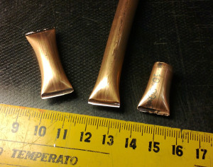
Here's how the crimped tubes look like. The first test resulted in a jagged edge, while the second test produced a nice straight cut. We will test how vacuum-tight these are with a Helium sniffer later.

13040022

PDF drawings:

A White Rabbit test

Update3: Here's what happens if you disconnect the master from the switch. The slave clock runs off on its own, with about 5ppm drift compared to the reference clock. Once the fiber is connected again it takes a few seconds to re-sync and lock on to the master clock.

wr_master_kuitu_irti

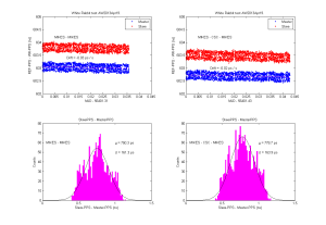
Update2: two different measurements, on the left with a short 2m fiber, and on the right with a few hundred meters of fiber to a WR-Switch, and a few hundred meters back.

wr_gm_test_csc_2013apr19

Update: an improved measurement now shows some promise:

wr_gm_test_2013apr19

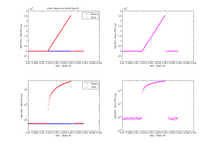
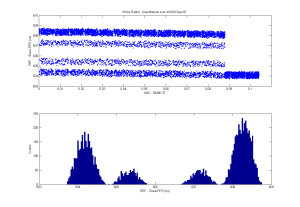
Testing White Rabbit at work. These are fancy network-cards connected by optical fiber which allow synchronization between the cards at better than 1 nanosecond level. My first results are a bit strange:

wr_grandmaster_short_fiber_slave-pps_stats

This is in "grandmaster" mode where we input a 1 PPS and a 10 MHz signal to one of the cards:

13040007

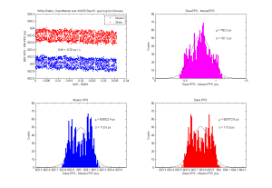
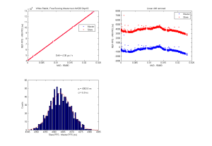
A second result in "free-running" master mode:

WR_freemaster_pps_stats


Strontium Blues

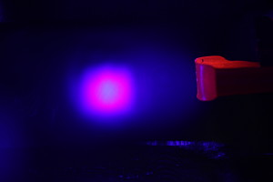
We've been playing with a blue laser at 461 nm in the lab lately. If tuned to just the right frequency (wavelength) neutral Strontium atoms will strongly absorb the laser light. Shortly (5 nanoseconds) after that the atoms emit at 461nm also, allowing us to see them:

strontium_461

The atoms originate from a hot "oven" at the right. It glows dark red because it's heated by driving a 5 A to 7 A current through it. The cloud of absorbing atoms glows at 461nm in the centre of the picture.

We can scan the laser frequency by adjusting the current through the diode-laser that produces the light. If the frequency is too low or too high we'll see nothing as the light will just pass through the cloud of atoms without interacting. On each side of the correct absorption frequency we'll see different parts of the atom cloud light up. This happens because the atoms stream out of the oven in slightly different directions, so they experience a different Doppler shift and will react to light with a wavelength slightly to the blue or red from the centre of the absorption-line at 461nm.

When slowly scanning the laser frequency over the absorption-line we got these nice videos. One with a narrow beam and one where the laser beam was expanded.

These were shot with a Canon DSLR so be sure to view them in HD on youtube!

TEC mount for laser-module

tec_adapter_1

tec_adapter_2

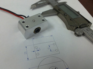
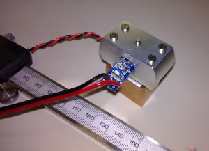
I made this aluminium bit on the lathe/mill today. It holds a blue laser-module from dealextreme. The brass barrel measured about 11.81 to 11.84 mm in diameter so I first drilled a 10mm hole, then opened it up slowly on the lathe until the module just fit the hole. There is an M3 set-screw to hold the laser module in place. Four long M2.5 screws clamp the aluminium part into contact with a peltier-element and the copper heatsink. A thermistor for temperature measurement and feedback control will be glued to the aluminium part as close as possible to the peltier.

Temperature control of the laser diode should provide for rough tuning of the laser wavelength. We want the wavelength to be about 405.2 nm, to be used for photoionization of Strontium.

Aside: A few years ago I tried to order some of these 405nm laser-pointers to the university. It was impossibly difficult because the shipments were stopped by the customs. Negotiations with the radiation-safety authorities did not help. It's simply forbidden to import non CE-approved laser-pointers - it doesn't matter if you are a researcher or work at a research institution. The story is completely different for laser modules (this is exactly the same product as the laser-pointer, but without the pen-like shape and the battery holder). Apparently these are classified just as "diodes" or "electronic components" and there are no problems getting them through customs.